Research

Silicon Electrochemical Micromachining (ECM) Technology
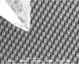
The fabrication of very high aspect-ratio silicon microstructures (e.g. pillars, trenches, etc.) and microsystems (e.g. M(O)EMS, gripper, etc.) with arbitrary shape at low cost is of relevance for a multitude of hot research topics and commercial applications, such as, energy harvesting, Lab-on-Chip fabrication, 3D microchip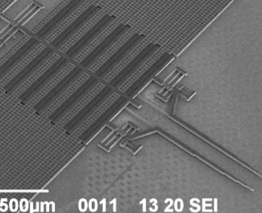 stacking.
This projet is aimed at the continuous development of the ECM technology to enable the low-cost fabrication of both microstructures of various shape and microsystems of high complexity with sub-micrometric accuracy at aspect-ratio values (over 100) not attainable from up-to-date bulk silicon micromachining technologies.
Researchers: L. M. Strambini, C. Cozzi, G. Polito, V. Robbiano
Funding ID: STMicroelectronics, Italian Minister for University and Research, EC-H2020
Recent key publications:
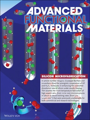
- C. Cozzi, G. Polito, K. Kolasinski, G. Barillaro, Controlled Microfabrication of High-Aspect-Ratio Structures in Silicon at the Highest Etching Rates: The Role of H2O2 in the Anodic Dissolution of Silicon in Acidic Electrolytes, Advanced Functional Materials (2016). [pdf][link]
- M. Bassu, S. Surdo, L. M. Strambini, G. Barillaro, Electrochemical micromachining as an enabling technology for advanced silicon microstructuring, Advanced Functional Materials, 22 (6), 1222-1228 (2012). [pdf]
Research activities are mainly focused to novel microstructured and nanoctructured materials, devices and systems for applications ranging from nanomedicine to biosensing, from microelectronics to photonics.
Minimally invasive microneedles for pain-free trasndermal monitoring of analytes of clinical interest
A novel trend is rapidly emerging in the use of microneedles, which are a miniaturized replica of hypodermic needles with length-scales of hundreds
of micrometers, aimed at the transdermal biosensing of analytes of clinical interest, e.g., glucose, biomarkers, and others
This project is aimed at the development and testing of microneedle patches for monitoring of analytes of clinical interest in the outer layers of the skin, e.g. glucose, so as to provide patients with a minimally-invasive and pain-free (bio)sensing system.
Researchers: L. M. Strambini, L. Ventrelli, S. Mariani
Funding ID: Tuscany Region, Italian Minister for University and Research
Recent key publications:
- L. Ventrelli, L. M. Strambini, G. Barillaro, Microneedles for Transdermal Biosensing: Current Picture and Future Direction, Advanced HealthCare Materials (2015) [pdf] [link]
- L.M. Strambini, A. Longo, S. Scarano, T. Prescimone, I. Palchetti, M. Minunni, D. Giannessi, G. Barillaro, Self-Powered Microneedle-Based Biosensors for Pain-Free High-Accuracy Measurement of Glycaemia in Interstitial Fluid, Biosensors and Bioelectronics (2014). [pdf]
- L. M. Strambini, A. Longo, A. Diligenti, G. Barillaro, A Minimally Invasive Microchip for Transdermal Injection/Sampling Applications, Lab on a Chip, 12, 3370-3379 (2012).
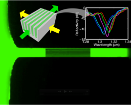
Optofluidic photonic crystal microsystems for chemical/biomedical applications
There is an increasing research trend for the fabrication of a novel generation of drop-and-measure optofluidic microsystems (OFMs) for label- free biological/chemical analysis that integrate materials with unique optical properties in microfluidic systems, among which photonic crystals are an example.
Researchers: L. M. Strambini, S. Mariani
Funding ID: Italian Minister of University and Research
Recent key publications:
- S. Surdo, F. Carpignano, L. Strambini, S. Merlo, G. Barillaro, Capillarity-Driven (Self-Powered) One-Dimensional Photonic Crystals for Refractometry and (Bio)sensing, RSC Advances, 4, 51935 (2014). [pdf]
- S. Surdo, S. Merlo, F. Carpignano, L. M. Strambini, C. Trono, A. Giannetti, F. Baldini, G. Barillaro, Optofluidic microsystems with integrated vertical one-dimensional photonic crystals for chemical analysis, Lab Chip, 12 (21), 4403 - 4415 (2012). [pdf]
Meso/nanostructured porous silicon for sensing/biosensing applications
A significant part of the research and development in the gas sensor field is currently devoted to sensor miniaturization and integration. This task requires the development of both sensitive layers and sensor structures compatible with integrated circuit (IC) fabrication processes. Old and new materials such as polymers, thick and thin metal oxides, porous silicon (PS), carbon nanotubes, and others are today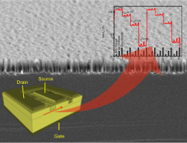 under investigation. The sensor miniaturization enables the fabrication of integrated sensing platforms, for example by using the CMOS leading technology, containing chemical sensors together with the related driving/readout electronics on a single chip.
This project has the main aim of developing novel integrated sensors/biosensors, by modification of solid-state electronic devices using meso/nanostructured porous silicon, to be integrated on the same silicon chip with electronic driving/readout circuits for the realization of miniaturized CMOS sensing platforms.
Researchers: L. M. Strambini
Funding ID: Italian Minister of University and Research, Tuscany Region
Recent key publications:
-
-Chemi-Transistor Sensors Based on Composite Porous Silicon/Gold Nanostructures Prepared by Metal-Assisted Etching, ACS Applied Materials and Interfaces 7, 7136 (2015). [pdf]
-
-G. M. Lazzerini, L. M. Strambini, G. Barillaro, Addressing Reliability and Degradation of Chemitransistor Sensors by Electrical Tuning of the Sensitivity , Nature Scientific Reports, 3, 1161 (2013). [pdf].
3D microincubators for evaluating the metastatic potential of tumor cells
The recent progress in cell culture and microfabrication technologies has suggested the development of cell-based sensors for drug discovery, clinical diagnostics, and detection of toxic agents. Cell-based biosensors are devices that contain living cells as bioreceptors and allow cell morphofunctional changes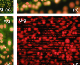 and/or detachment, induced by exposure to environmental perturbations, to be monitored by a suitable transduction (i.e., optical, electrical) method. Cells, as bioreceptors, convert the presence/action of a bioactive agent into a cellular signal; the transducer converts the resulting cellular response into an electric or optical signal that can be processed and analyzed, possibly in a noninvasive manner.
This project carried out with Prof. S. Merlo of University of Pavia and Dr. G. Mazzini CRN-IGM Pavia, is aimed at the development of 3D microincubators for cell cultures also acting as label-free optical transducers, with the aim of evaluating the metastatic potential of tumor cells.
Researchers:
Funding ID: Italian Minister of University and Research, Fondazione Alma Mater Ticinensis, Fundazione Cariplo
Recent key publications:
- G. Mazzini, F. Carpignano, S. Surdo, F. Aredia, N. Panini, M. Torchio, E. Erba, M. Danova, A. I. Scovassi, G. Barillaro, S. Merlo, 3D silicon microstructures: a new tool for evaluatingbiological aggressiveness of tumour cells, IEEE Transactions on NanoBioscience (2015). [pdf]
- F. Carpignano, G. Silva, S. Surdo, V. Leva, A. Montecucco, F. Aredia, A. I. Scovassi, S. Merlo, G. Barillaro, G. Mazzini, A new cell-selective three-dimensional microincubator based on silicon photonic crystals, PLoS One, 7(11), e48556 (2012). [pdf]
Light-activated highly conformal deposition of microstructured polymer films
Conducting polymers (CPs) have been demonstrated to possess in- teresting properties for applications in different fields, from electronics, chemical sensors to energy storage and surface coatings. Recently, great efforts have been devoted to the development of technologies for the 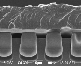 fabrication of micro/nanostructured CPs-based devices taking advantage of CP features at the micro/nanoscale, mainly related to larger surface area and three-dimensional (3D) arrangement of polymer chains as compared to bulk material.
This project, carried out in collaboration with Dr. E. Mazzotta of University of Salento, has the aim of setting up a novel light-activated electrosynthesis of microstructured CP films on microstructured silicon templates for the fabrication of CP-based devices for sensing/biosensing applications.
Researchers: S. Surdo
Funding ID: University of Salento, Italian Minister for University and Research
- E. Mazzotta, S. Surdo, C. Malitesta, G. Barillaro, High-aspect-ratio conducting polymer microtube synthesis by light-activated electropolymerization on microstructured silicon, Electrochemistry Communications 35, 12 (2013). [pdf]
- Recent key publications: S. Surdo, L.M. Strambini, C. Malitesta, E. Mazzotta, G. Barillaro, Highly Conformal Growth of Microstructured Polypyrrole Films by Electrosynthesis on Micromachined Silicon Substrates, Electrochemistry Communications, 14, 1-4 (2012). [pdf]