Pennelli's Research

Giovanni Pennelli: RESEARCH


THERMOELECTRIC DEVICES

Heat is energy. Cheap, compact and reliable devices capable of a direct conversion of heat into electrical power will have a strong impact on the field of the green energy harvesting.
Selected publications:

Pennelli Giovanni.
Review of nanostructured devices for thermoelectric applications.
BEILSTEIN JOURNAL OF NANOTECHNOLOGY, 5:1268-1284, 2014.
[DOI | .pdf ]

Pennelli Giovanni.
Top-down fabrication of silicon nanowire devices for thermoelectric applications: properties and perspectives.
THE EUROPEAN PHYSICAL JOURNAL. B, CONDENSED MATTER PHYSICS, 88, 2015.
[DOI |http ]


THERMOELECTRIC DEVICES:
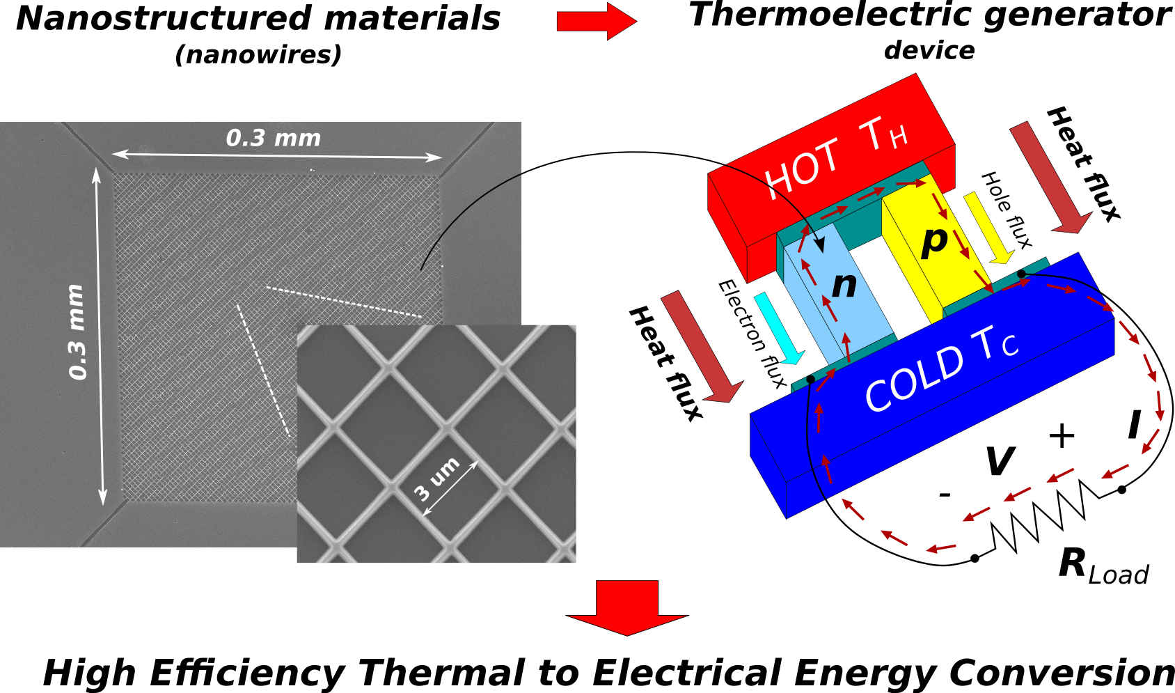
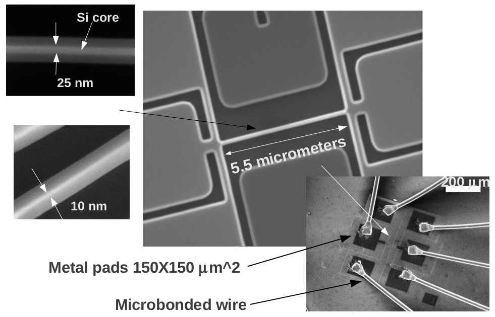
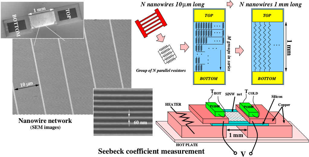
Interconnected silicon nanostructures for thermoelectricity

Devices based on large arrays of silicon nanowires and nanomembranes for thermal to electrical energy conversion.
Selected publications:

Pennelli G, Totaro M, Piotto M, and Bruschi P.
Seebeck coefficient of nanowires interconnected into large area networks.
NANO LETTERS, 13:2592-2597, 2013. [DOI ]

Pennelli G and Macucci M.
High-power thermoelectric generators based on nanostructured silicon.
SEMICONDUCTOR SCIENCE AND TECHNOLOGY, 31:1-8, 2016. [DOI | http ]


THERMOELECTRIC DEVICES:
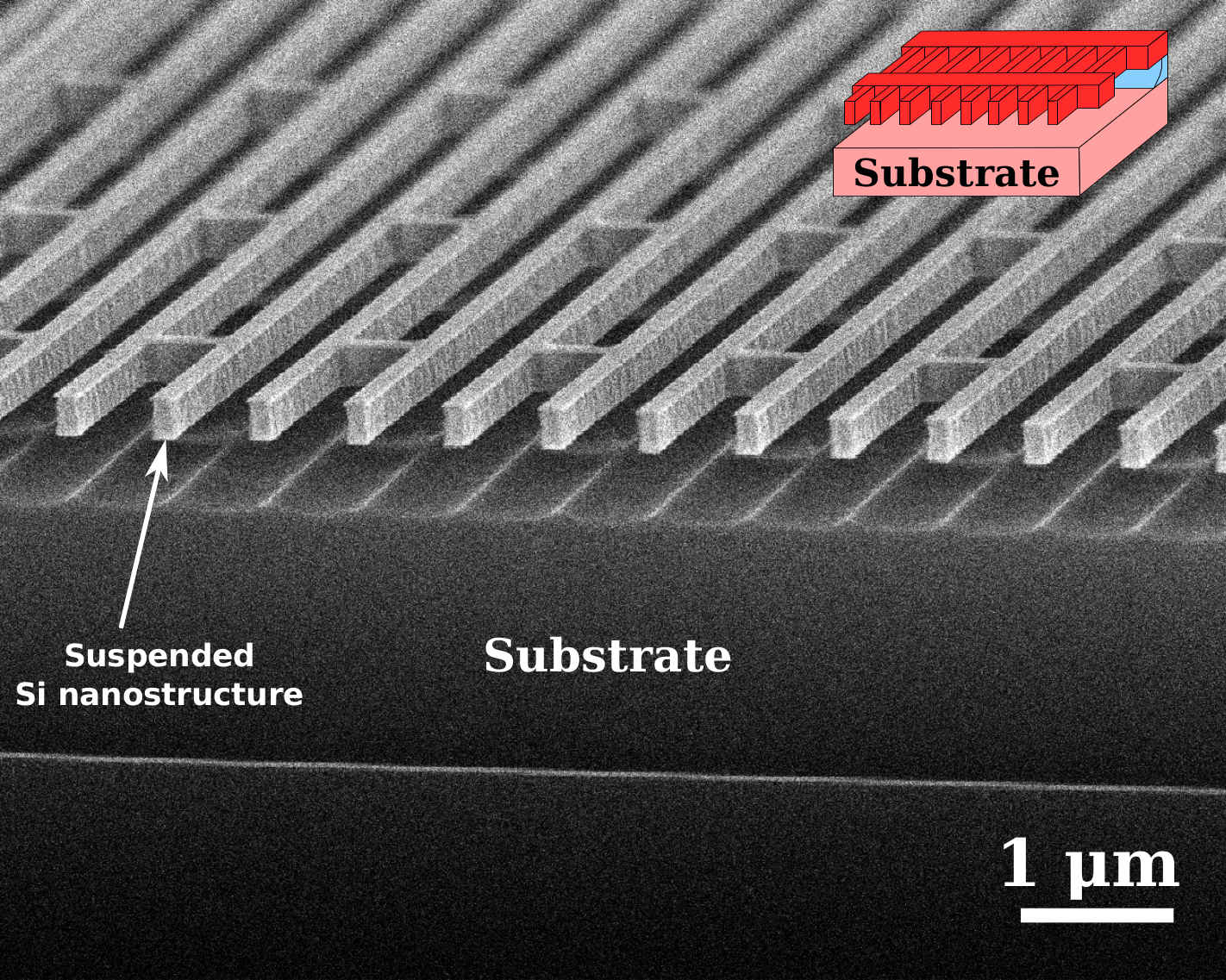
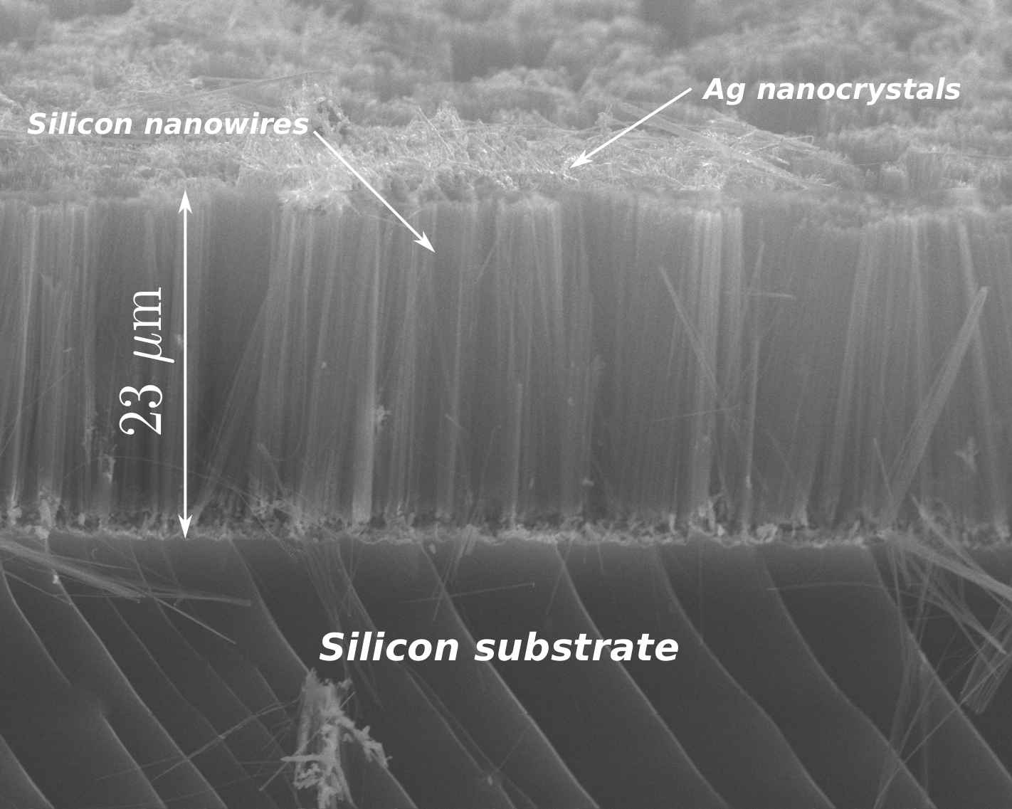
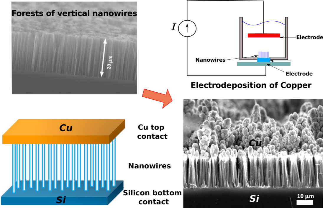
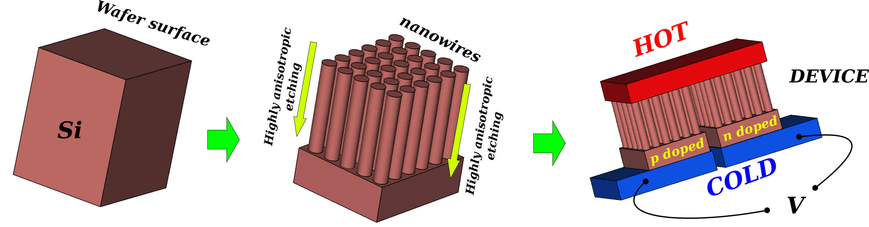
Silicon nanowire forests for thermoelectricity

Vertical nanowires are fabricated by means of Metal Assisted Silicon Etching. A top contact is provided by a thick copper layer, deposited by electrodeposition.
Selected publications:

E.Dimaggio, G.Pennelli
Reliable fabrication of metal contacts on silicon nanowire forests.
NANO LETTERS, 16:4348-4354, 2016. [DOI |http ]


SILICON NANOJUNCTION DEVICES

A process for opening very narrow windows through the oxide surrounding the silicon nanowires has been developed. Selective doping is possible. A gate almost all around the nanowire has been fabricated, and JFET characteristics have been measured.

Selected publications:

Pennelli G, Totaro M, and Piotto M.
Selective doping of silicon nanowires by means of electron beam stimulated silicon dioxide etching.
NANO LETTERS, 12:1096-1101, 2012. [ bib ]

Pennelli G and Piotto M.
Metal nanojunctions on silicon single nanowire devices.
9TH IEEE CONFERENCE ON NANOTECHNOLOGY (IEEE-NANO), 2009. [ bib ]


SILICON NANOWIRE DEVICES

Processes for the top-down fabrication of devices based on a single (or very few) nanowires have been developed and improved. The reliable fabrication of nanowires as small as 10 nm has been demonstrated.

Selected publications:

Pennelli G. and Pellegrini B.
Fabrication of silicon nanostructures by geometry controlled oxidation.
JOURNAL OF APPLIED PHYSICS, 101:10450-10458, 2007. [DOI ]

Pennelli G. and Piotto M.
Fabrication and characterization of silicon nanowires with triangular cross section.
JOURNAL OF APPLIED PHYSICS, 100:054507-1-054507-9, 2006. [DOI ]

Pennelli G.
Top down fabrication of long silicon nanowire devices by means of lateral oxidation.
MICROELECTRONIC ENGINEERING, 86:2139-2143, 2009. [DOI ]


HIGH RESOLUTION ELECTRON BEAM LITHOGRAPHY

The hardware and software of an innovative system (pattern generator) for electron beam lithography has been developed and tested. The system allows the fabrication of features smaller than 10 nm.

Selected publications:

Pennelli G.
Fast, high bit number pattern generator for electron and ion beam lithographies.
REVIEW OF SCIENTIFIC INSTRUMENTS, 79, 2008. [DOI ]

G PENNELLI, A DANGELO, G BARILLARO, M PIOTTO, and PELLEGRINI B.
A low cost high resolution pattern generator for electron-beam lithography.
REVIEW OF SCIENTIFIC INSTRUMENTS, 74 (7):3579-3582, 2003. [DOI ]